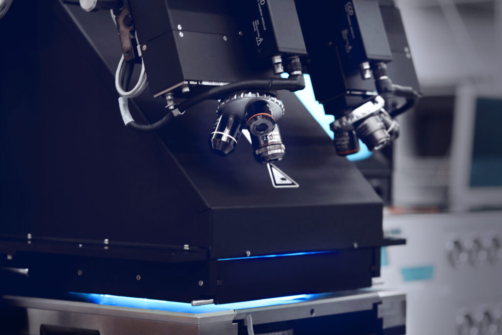
THIN FILM DEPOSITION
A wide range of metallic or insulating materials are available for use thanks to our PVD and PECVD thin layer vacuum deposition techniques. The substrates or supports can be silicon, glass or sapphire…
PVD (Physical Vapor Deposition):
- Available materials: aluminum (Al), copper (Cu), gold (Au), 5N gold, chromium (Cr), titanium nitride (TiN).
- Deposited thickness : from a few nanometers to 1 micron.
- On substrates up to 200 mm in diameter.
- Possibility of processing smaller parts collectively.
PECVD (Plasma-Enhanced Chemical Vapor Deposition):
- Available materials : silicon oxide (SiO2), silicon nitride (SiN).
- Deposited thickness : from a few nanometers to 1 micron.
- On substrates up to 200mm in diameter.
- Possibility of processing smaller parts collectively.


HIGH RESOLUTION PHOTOLITHOGRAPHY
We apply a mask to the substrate containing the desired design information. We can process your files from a .jpeg, .png, .tiff, .ai, .pdf format… in order to print them on the desired media. It is also possible to align with existing patterns with micron accuracy.

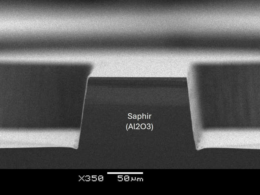
NANO-ETCHING
We engrave the material through the mask made during the photolithography step. The design is thus transferred to the underlying layer or to the substrate. The fineness of the engraving line can reach 2µm, which gives this technique many advantages:
- Creation of visual effects: iridescence, opacity gradients, “smoky” effect.
- Miniaturization of electronic devices.
- Deep etching of several tens of micrometers in the sapphire without residual roughness.

